Resistor chart.
Torroid (iron powder & ferrite) info.
Transister stuff:
| Transistor Pinouts | ||
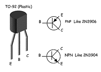 Here's a very common plastic package; the TO-92. Beware, not all parts
in TO-92 share this pinout. Here are some that do:
Here's a very common plastic package; the TO-92. Beware, not all parts
in TO-92 share this pinout. Here are some that do:
|
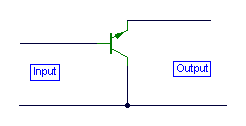
There are plenty of texts around on basic electronics, so this is a very brief look at the three basic ways in which a bipolar junction transistor (BJT) can be used. In each case, one terminal is common to both the input and output signal. All the circuits shown here are without bias circuits and power supplies for clarity.
Common Emitter Configuration
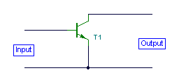
Here the emitter terminal is common to both the input and output signal. The arrangement is the same for a PNP transistor. Used in this way the transistor has the advantages of a medium input impedance, medium output impedance, high voltage gain and high current gain.
Common Base Configuration
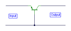
Here the base is the common terminal. Used frequently for RF applications, this stage has the following properties. Low input impedance, high output impedance, unity (or less) current gain and high voltage gain.
Common Collector Configuration
This last configuration is also more commonly known as the emitter follower. This is because the input signal applied at the base is "followed" quite closely at the emitter with a voltage gain close to unity. The properties are a high input impedance, a very low output impedance, a unity (or less) voltage gain and a high current gain. This circuit is also used extensively as a "buffer" converting impedances or for feeding or driving long cables or low impedance loads.
A note on Phase Shifts
In both the the common emitter and emitter follower configurations, the input
and output signals are out of phase by 180 degrees. This is not a phase displacement,
but a phase inversion. The common base mode however tracks the input and output
with 0 degrees phase shift.
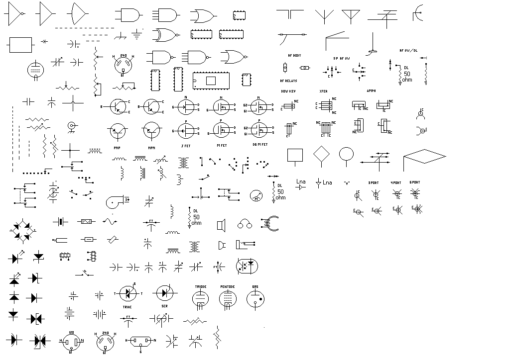
Transistor / IC / Diode layout.